Electro-optics is the technology that uses electrical signals to control optical properties. It is one of the most useful areas of photonics.
In this article, you will learn about why electro-optics is important as well as how it is used in various photonic applications.
Why are electro-optic effects so important?
Electricity and electronics absolutely dominate technology as we know it today.
Several optical materials are passive – they have fixed optical properties e.g. absorption, refractive index, etc.
In contrast, the optical properties of some materials can be controlled with an electrical signal.
It is no surprise then that electricity and electronics play a central role in optics and photonics.
As a matter of fact, electro-optics is the “bridging technology” between electronics and photonics. It is a hybrid technology which combines the best aspects of electricity and light.
In a previous blog post, the special relationship between electronics and photonics is discussed in depth.
In this report, the focus is on a hybrid technology which combines the best aspects of electricity and light for everyday applications.
Isotropic vs anisotropic optical media
Electro-optic effects have a lot to do with symmetry. Materials can be classified according to the optical symmetries they can harness.
Accordingly, materials used in optics and photonics fall into one of two broad classes: isotropic or anisotropic optical materials.
In isotropic materials, there is no preferred direction since the refractive index is the same whichever way you “look”. Examples of isotropic optical media include vacuum, air and glass.
Light travels in air (refractive index = 1) at 3 x 10⁸ m/s i.e. covering a distance of 30 cm every nanosecond irrespective of the direction in which it travels.
In glass (refractive index = 1.5), light travels at only 2 x 10⁸ m/s i.e. covering a distance 20 cm every nanosecond. This is only 67% of its speed in air!
In anisotropic optical materials, light feels a different refractive index for different directions.
For example, for the nematic liquid crystal mixture E7, the refractive index varies between two extremes.
At the telecom wavelength of 1550 nm, these are the ordinary refractive index (no = 1.5) and the extraordinary refractive index (ne = 1.72).
This means different light polarizations may “see” a different refractive index in an anisotropic material.
This is the origin of interesting phenomena like double refraction which occurs in some materials e.g. calcite.
Optical anisotropy offers interesting engineering possibilities.
If you can find some clever way to control the refractive index “seen” by different light polarizations, you can build very powerful devices.
Useful photonics applications become possible when the refractive index and hence polarization state of light can be controlled precisely by applying an electric field over an electro-optic material.
In the next section, we look at a number of important electro-optic effects.
What are the main electro-optic effects?
In this section, I take you through the main electro-optic effects.
Electrochromic effect
Electrochromism is the change in a material’s color or opacity when an electric field is applied to it.
Electrochromic materials exhibit a persistent change in color i.e. the electric field only needs to be applied once to cause a change in color.
Electrochromic materials with electrically controlled opacity to infrared light are excellent candidates for use as smart windows.
Smart windows can lead to more energy-efficient buildings since they reduce the amount of energy needed to heat up a building during winter or cool it down during summer.
Smart windows are also used in cars and aircraft. For example, the picture below shows an electrochromic window in a Boeing 787.

Electro-absorption effect
The electro-absorption effect occurs when an optical material’s absorption changes when an electric field is applied to it.
In semiconductors, electro-absorption is known as the Franz-Keldysh effect.
The Franz-Keldysh effect arises in semiconductors because the applied electric field modifies the band gap.
In layered semiconductor devices like quantum wells, the electro-absorption effect is also known as the quantum confined Stark effect.
A quantum well is made by growing alternating layers of semiconductor materials with different band gaps.
One of the simplest examples of a quantum well is formed when a thin layer of gallium arsenide is sandwiched between two layers of aluminum gallium arsenide.
Quantum wells make it possible to precisely engineer the band gap of the semiconductor material.
Precise control of the band gap allows engineers to design devices such as electro-optical modulators, switches as well as saturable absorbers.
The Pockels (linear electro-optic) effect
In materials that exhibit the Pockels effect, the change in refractive index is proportional to the applied electric field.
In order for a material to exhibit this behavior, it must have a crystal structure that lacks inversion symmetry.
Physically, a lack of inversion symmetry means the material’s crystal structure is not the same in every direction when looking from a reference point chosen at random.
Potassium Dihydrogen Phosphate and Lithium Niobate are examples of materials which lack inversion symmetry.
The Kerr (quadratic electro-optic) effect
The Kerr effect occurs when a material’s refractive index changes proportionally to the square of the applied electric field.
Since light is an electromagnetic wave, it has electric and magnetic field components oscillating orthogonal to each other.
When the electric field is strong enough, then we get the optical Kerr effect.
The refractive index of the material then changes proportionally with the intensity of the light (which is itself proportional to the square of the electric field).
All materials have a Kerr coefficient. However, it is usually much smaller than the Pockels coefficient.
Use cases of electro-optic materials
In the previous section, you learned about the various optical effects that can be induced by an applied electric field.
In this section, you will be introduced to a selection of practical use cases for electro-optic materials and devices in photonics.
Devices based on liquid crystals
Liquid crystals (LCs) are probably one of the most widely used electro-optic materials.
LCs are organic materials which are usually used at a temperature whereby they are in the liquid phase.
The constituent molecules of LCs have an elongated or rod shape.
When a sufficiently high voltage is applied to a thin LC layer, its molecules respond by aligning themselves in such a way as to minimise their free energy.
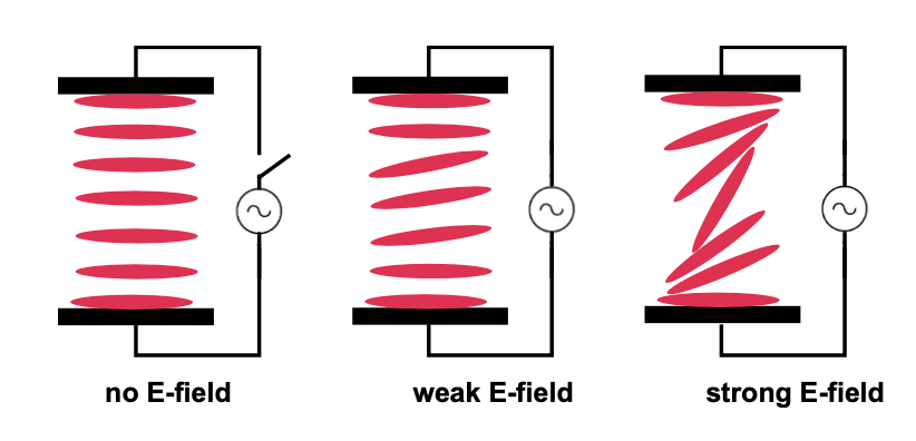
A practical LC device is typically created by infiltrating the LC molecules into a gap between two (usually) glass plates to form an LC cell.
The voltage is applied to the LC layer by means of transparent electrodes deposited on the glass plates.
The voltage applied to the LC layer effectively controls the properties of the light travelling through it. This can be used in a number of interesting ways in everyday appliances.
For example, in an LCD/LED display or TV, individual pixels are switched on or off by switching an LC layer sandwiched between crossed-polarizers with a moderate voltage.
The electrodes on the glass plates making up the LC cell may be patterned in creative ways in order to actively control the spatial distribution of the wavefronts of a light beam.
This is used in application such as LC lenses with adjustable focus and spatial light modulators for advanced beam-shaping.
LC layers may also be deposited on passive components like integrated photonic waveguides or ring resonators in order to precisely control the light guided in them.
In this case, the guided modes of a waveguide feel the refractive index in the cladding.
The guided modes of the waveguide can be tuned by applying a moderate voltage over the LC layer.
This is very attractive since it allows indirect electric control of an optical waveguide.
Thereby opening up possibilities for electrically controlled modulation, switching and routing of optical signals in photonic chips.
Electro-optic modulators
Electro-optic modulation is probably the most common kind of electro-optic application.
An electro-optic modulator is essentially a voltage-controlled waveplate. It usually consists of a birefringent crystal sandwiched between two electrodes.
It is of course necessary to arrange these electrodes such that there is an opening for light to enter and leave the crystal.
Electro-optic modulators can operate as either phase, polarization, or intensity modulators.
In order to achieve phase modulation, an electro-optic modulator uses an electric field to adjust the optical phase or retardation of orthogonal light polarisation as it travels through it.
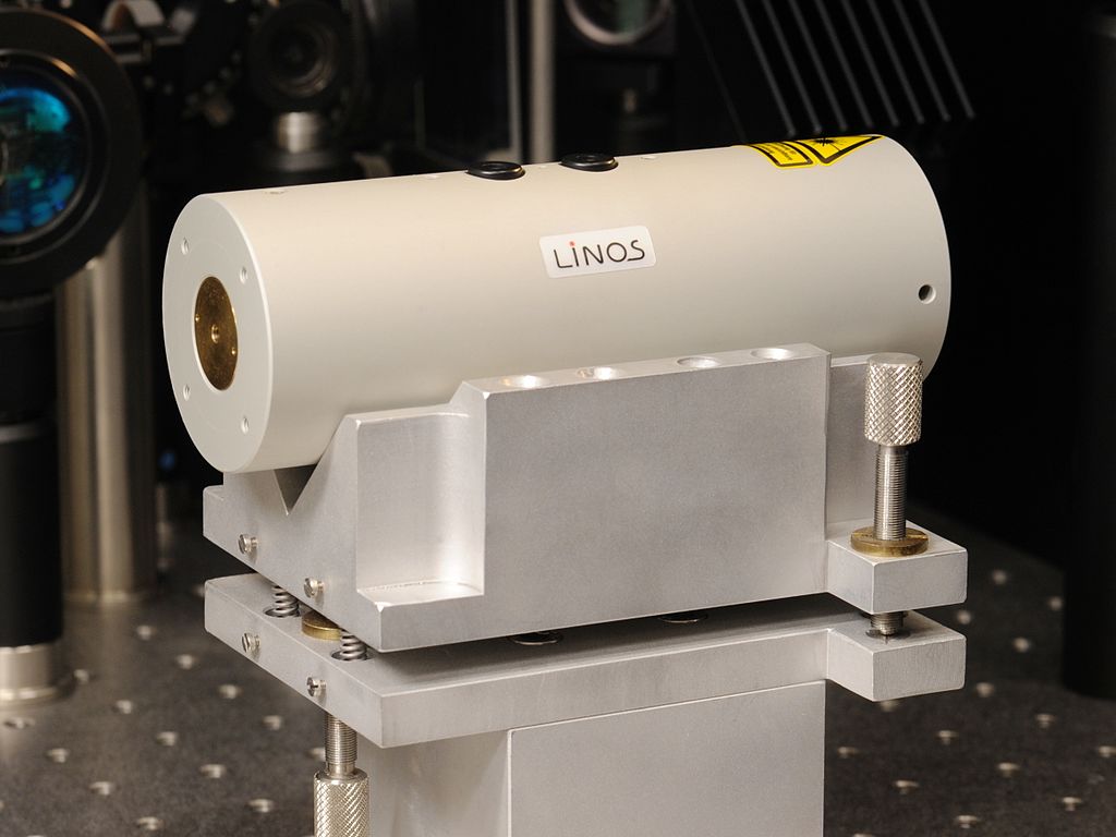
A popular example of an electro-optic modulator is the Pockels cell which is an electro-optic cell comprising a crystal without inversion symmetry sandwiched between two electrodes.
Examples of such crystals include Potassium Dihydrogen Phosphate and Lithium Niobate.
Pockels cells are attractive because they exhibit a linear relationship between change in refractive index and applied electric field.
A Pockels cell allows for precise control of the relative phase delay between two perpendicular polarization states by electrical means.
This makes them ideal for use in laser technology for mode-locking and Q-switching.
Conclusion
Electro-optic effects are a fascinating phenomenon that allows for the manipulation of light using electric fields.
These effects have a wide range of potential applications, and as further research goes on, expect to see even more interesting and useful application utilising electro-optic materials.
I like what you guys are up too. This kind of clever work and coverage! Keep up the great works guys I’ve included you guys to our blogroll.
Your blog is a true hidden gem on the internet. Your thoughtful analysis and engaging writing style set you apart from the crowd. Keep up the excellent work!