Photonics is concerned with the control of photons.
As a technology, photonics focuses on manipulating light to achieve some practical goals like telecommunication, sensing, industrial processing etc.
In photonics, photons are controlled in many ways e.g. switching, re-routing, modulation and amplification.
As semiconductors have become more important in optics, we have seen the emergence of hybrid fields where electronics and light come together.
For example, we have electro-optics: devices with electrically controlled optical behaviour e.g. liquid crystal displays (LCD).
Another is optoelectronics: electrical devices which actively interact with light e.g. light emitting diodes (LED).
Photonics vs electronics
There are other fields which come to mind too, for example, quantum electronics. We also increasingly have situations where electronic and optical functions are integrated into the same chip.
Electronics is the science of controlling electrons. The term photonics was coined as an analogous term for the technology related to controlling light.
Nowadays, semiconductors are the material of choice for both photonics and electronics.
Electrons propagating in a semiconductor can change its optical properties.
The reverse is also true – optical effects can change the electrical properties of a semiconductor. This confirms a fundamental link between electronics and photonics.
You can read more about this in our report on the fascinating relationship between photonics and electronics.
Photonics vs optics
In addition to its close connection to electronics, photonics shares an even stronger bond with optics. In fact, both terms are used interchangeably sometimes.
Optics as a discipline is almost 400 years old. Its origins can be traced back to the time when we developed some understanding of the nature of light.
Incremental advances in optics led to a better understanding of light which was then applied to the inventions of various types of optical instruments.
Starting from simple lenses and eventually lens assemblies, it was possible to invent devices like magnifying glasses, (fresnel) lenses for lighthouses, microscopes, telescopes etc.
A brief history of photonics
Optics can be seen as photonics 1.0. At its origins, it did not really concern itself with light generation.
Rather it focused on developing a sound theoretical basis and then using this to create practical innovations.
This latter part is similar to what photonics is doing today – taking advantage of solid theoretical foundations to develop advanced devices with practical applications.
Optics has mostly concerned itself with how to control the propagation of visible light as well as understanding light-matter interactions.
In the late 19th century, Maxwell showed light was an electromagnetic wave. He also confirmed the connection between light, electricity and magnetism.
This set the scene nicely for Albert Einstein to theorise about the existence of the laser a few decades later.
The early part of the 20th century saw advances in several related areas of physics.
Putting these together with the understanding of light as an electromagnetic wave led to the invention of devices like the light emitting diode (LED) and lasers by the middle of the 20th century.
These developments paved the way for photonics to “blast off” as a full-fledged discipline from the 1980s onwards.
Now since optics preceded photonics, it seems logical to conclude that the latter is a sub-field of the former.
In the last decade, we have seen this notion turned on its head as advances in photonics have sometimes required a drastic rethink of optics principles.
For example, over the last decade, we have seen advances in photonics requiring meta-materials.
Rather than letting material properties of naturally occurring optical materials determine what is technically possible, you instead start by identifying a desirable optical property or behaviour.
You can then engineer artificial materials with meta-atoms which can realise this behaviour.
One example of such exotic optical behaviour is the invisibility cloak which is well understood today and has been demonstrated experimentally.
Why do we need photonics?
The world as we know it today is driven by technology.
Our aspirations for the future – self-driving electric vehicles, the internet of things, 5G mobile connectivity, unlimited data transfer speeds for the internet, clean renewable energy, quantum computing, personalised medicine, industrial automation, space exploration etc – will all rely on advancements in some core technology.
Right now, this core technology is electronics.
Precise control of electron flow through billions of transistors contained in tiny integrated circuits is at the heart of modern technology.
Each new iteration of electronic integrated circuits can contain even more transistors than the previous one.
Practically, this means the computing power of electronic chips increases with each iteration with a corresponding reduction in their unit cost.
This is more or less the essence of Moore’s law which states that the number of transistors in an electronic chip doubles every (roughly) two years while the price halves.
According to Moore’s law, we should get more powerful and cheaper electronic chips as the years roll by.

Despite a successful track record going back about 60 years, Moore’s law can’t continue forever.
At least not with electronics as it is known today. In fact, Moore’s law is already “slowing” down as it is.
Right now the trick used by the electronics industry to increase the computing power of chips involves shrinking the critical dimensions of transistors.
At the moment, this figure is on the order of a few tens of nanometers; quite a remarkable achievement if you think about it.
Unfortunately, there is a physical limit to how small a transistor can be.
It is quite evident that at some point we have to come up with some new trick(s) to keep Moore’s law going. Photonics is the technology which can take over from electronics.
On a basic level, we can immediately appreciate photonics’ appeal by considering that it uses photons to perform computations.
Photons can travel a lot faster than electrons inside semiconductors. So the potential advantages are self-evident.
However, the photon’s speed is not the main differentiating factor between photonics and electronics. Information propagates as electromagnetic waves in both electronic and photonic systems.
Rather there are other factors which will eventually tip the balance in photonic’s favour:
No need to reinvent the wheel
Photonic integrated circuits are implemented using the same semiconductor fabs which are currently used to manufacture electronic chips.
This means huge capital equipment investments are not needed to switch from electronics to photonics.
This is a key economic aspect which cannot be overstated.
Light has desirable properties
Semiconductor materials like silicon have transparency windows for certain wavelength bands of light.
Light with wavelength falling within these bands can propagate with minimal loss in waveguides made out of glass or silicon.
There are no joule heating losses as we know it when electrons travel in a metal trace/wire.
The only losses are due to imperfections in the waveguide. Moreover, you have limited cross-talk between separate waveguides.
Additionally, with the proper design, you can also eliminate antenna effects which plague electronics.
Wavelength division multiplexing
Different wavelengths of light can be used as separate information channels on the same physical channel.
This technique makes it possible for photonic integrated circuits to attain speeds in the terabits per second (Tbps) range, well beyond the 100 gigabits per second (100 Gb/s) capability of current electronic circuits.
Photonics plays well with electronics
It is very unlikely to see photonics completely replace electronics overnight.
Rather, the most feasible way of phasing electronics out is to have hybrid electronic/photonic systems.
We already see examples of electronics chips augmented with photonics functionality.
An example of this is present-day application specific integrated circuits (ASICs) with optical buses which enable ultra-fast inter-chip communication between separate electronic chips.
Photonics is environmentally friendly
In an era when we think about clean sources of energy to safeguard our planet for future generations, photonics is a good pick.
We need a technology which consumes less energy.
It fits this narrative nicely since using light for computing requires much less energy than using electrons.
Photonics is an enabling technology
Photonics is an especially potent key enabling technology for the future. It finds applications in so many other fields.
Advances in photonics have a direct impact on sensor technology, machine vision and industrial manufacturing, medicine, telecommunications etc.
Global photonics market outlook
Now that we have covered the motivations behind our need for photonics and light technologies, we turn our sights to the market situation for photonics and light related technologies.
We first take a look at the market forecasts for the period between 2020 to 2025 and then move on to looking at estimated sizes for specific sectors.
It is quite difficult to get conclusive information on the forecasted revenues. There are several market research companies generating these forecasts.
They each make their own assumptions and rely on differing sources.
As such their forecasts are understandably different.
It is also quite difficult to get a complete picture of individual reports since most of these market forecast reports are hidden behind paywalls.
In the table below, I arrange some forecasted figures for the global photonics industry for the years 2020 through 2027. 2020 is the base year for all forecasts.
We have two forecasts running till 2025 and two others running till 2026 and 2027 respectively.
For each provider, the forecasted amount for each year is in billions of USD in the appropriate column.
The last column gives the cumulative annual growth rate (CAGR).
| Provider | 2020 | 2025 | 2026 | 2027 | CAGR |
| Research and Markets | 590.0 | 830.0 | – | – | 5,9% |
| Markets and Markets | 594.0 | 838.0 | – | – | 7,1% |
| Mordor Intelligence | 590.0 | – | 1,020.0 | – | 7,1% |
| StrategyR | 690.5 | – | – | 970.5 | 7.0% |
From the numbers shown here, we can conclude that the global photonics market will grow substantially with a CAGR of about 7% in the next coming years.
These figures are set to get even better by 2030 and beyond.
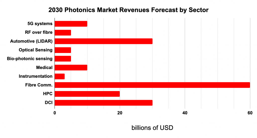
It is also instructive to take a look at specific sectors within the photonics business to get some feel for which areas are really pulling the industry ahead.
We immediately notice the leading position of fibre communications with forecasted revenues of 60 billion USD by 2030.
This is to be expected as it is arguably the first large-scale photonic application. It is set to continue in its leading position for the next few years at least.
Forecasts for Automotive (mostly driven by LIDAR for self-driving cars etc) and data centre interconnects (DCI) with 30 billion USD each as well as high-performance computing (HPC) with 20 billion USD reveal these sectors as key growth areas for the coming years.
Photonics research areas
Photonics as an engineering discipline relies heavily on quality research.
There is a lot of ongoing research which gets integrated into innovative devices and products which solve everyday problems.
In this section, we look at the sub-fields of photonics research which make it possible to accurately control light.
Light sources
One of photonics’ main goals is to create novel light sources for its broad range of applications.
The focus is on electrically controlled semiconductor light sources like light-emitting diodes (LEDs) and lasers.
There is a lot of research that goes into customising each LED or laser to fit its target application.
For instance, LEDs can be adapted to emit in different wavelength bands. A particularly interesting problem is that of producing white light with LEDs.
One approach involves using a blue or ultra-violet LED which illuminates a surface coated with a phosphor which then emits white light.
The other method involves using blue, red and green LEDs together. By mixing these three primary colours we get white light.
LEDs can also be engineered to switch on and off quite fast making them suitable as sources for simple optical networks.
Lasers are of course widely used in photonics.
There are several types – solid state, gas, liquid, Q-switched, soft-matter (e.g. low power liquid crystal lasers), vertical cavity surface emitting lasers (VCSELs) etc.
Nanophotonics
As the name implies this branch of photonics research is concerned with investigating how light interacts with components/devices realised in semiconductor materials which have critical dimensions comparable to that of light.
For context, remember visible light has wavelengths between 400 nm to 700 nm.
Light is mostly treated as a Gaussian beam here since the ray and geometrical approaches are no longer adequate.
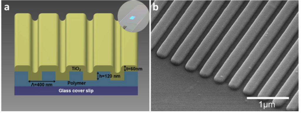
Nanophotonics includes research on all the components necessary to realise (silicon) photonic integrated circuits. Research interests include components like;
- waveguides for controlling on-chip propagation of light. There are various types e.g. ridge, rib and slot waveguides etc;
- grating couplers for coupling light into and out of waveguides;
- ring resonators and waveguide gratings for filtering light;
- arrayed waveguide gratings, multimode interference couplers for (de-)multiplexing light of slightly different wavelengths;
- Mach-Zhender interferometers;
- photonic crystals – photonic crystal fibres and photonic crystal waveguides;
- meta-materials – meta-lenses, meta-surfaces etc
Meta-materials are (as we mentioned earlier) another very active area of nano-photonics research.
These man-made materials can interact with light in sometimes very counterintuitive ways.
Recent really cool results include materials with a negative index of refraction and invisibility cloaking.
Photonics processing technology
Photonics typically requires lots of technology development to realise the devices it needs.
This is of course borrowing a lot from the microelectronics industry which has developed the technology for producing silicon wafers with amazing reliability and quality.
Photonics goes further, it usually requires lots of other materials with excellent properties when used on their own or combined with silicon.
For example, it is not possible to realise light sources in crystalline silicon since it has an indirect band gap. So it is usually necessary to integrate it with other materials with a direct band gap.
Excellent examples are III-V semiconductor materials like gallium arsenide (GaAs), indium arsenide (InAs), indium gallium arsenide (InGaAs) etc.
This means engineers have to find a means to integrate these materials together.
Accordingly, various technological processes are implemented like flip-chip bonding and epitaxy.
Epitaxy is especially interesting as it involves chemically growing layers of a material atom by atom. There are several parameters which can be controlled.
Epitaxial growth is frequently done in a vacuum and uses various gas mixtures.
There are many techniques used in epitaxy depending on the target applications. These include vapour phase epitaxy (VPE), chemical vapour deposition (CVD), and metal-organic chemical vapour deposition (MOCVD).
Photonic materials
In addition to semiconductors like silicon, various other materials are required for photonics.
The various aspects of photonics – light generation, control and detection – may sometimes require materials with very different properties.
Engineers are always looking for new and more efficient ways to accomplish these functions.
Light generation requires materials with can emit light in response to electrical stimulation.
As we mentioned earlier under light sources LEDs and lasers are the main ways to generate light for photonics. We have classic semiconductor LEDs and lasers.
Additionally, the same functions can be obtained in soft organic matter or polymers.
An excellent example of this is the class of polymers called organic light-emitting diodes (OLEDs).
Controlling light requires both passive and active materials.
The active materials are particularly interesting as they can change their optical properties due to some external stimulus.
This is the realm of “x – optic” materials where x represents the stimulus which causes the change in optical properties.
It is typically desirable to have a large optical change for a minimal stimulus signal/level. For example, we have:
Electro-optic materials
The optical properties of this type of material can be changed by applying an electric field to them.
Examples of this type of material include liquid crystals and lithium niobate.
Liquid crystals have long rod-shaped molecules that possess optical anisotropy i.e. the refractive index is dependent on the direction of light propagation.
When they are subjected to an electric field, their molecules reorient themselves to minimise their energy and align themselves with the electric field.
This is electrically controlled optical behaviour which is a very desirable property used in devices like displays and spatial light modulators.
Thermo-optic materials
The optical properties of these materials can be altered by regulating their temperature.
Materials with a liquid crystal phase are again excellent examples of thermo-optic behaviour.
This is an important aspect in most of photonics because device behaviour is frequently affected by temperature changes.
Most common photonic materials have a thermo-optic coefficient which either needs to be accounted for or taken advantage of.
For example, most photonic integrated circuits utilise thermo-optic phase shifters.
Other materials
It is also worthwhile to mention photonics research has also identified various other materials whose optical characteristics can be altered by varying some other physical quantity e.g piezo-optic (pressure), acousto-optic (sound) and elasto-optic (elasticity).
Quantum photonics
Quantum photonics focuses on investigating photonic devices which operate in a regime where quantum effects are important.
The end game is to realise integrated quantum photonic circuits for future quantum communication and information processing applications.
There is serious research going on in this area and some pieces of the puzzle like single photon sources are already practically realised.
Bio-photonics
Bio-photonics is a branch of photonics research aiming to apply photonics techniques to medicine and the life sciences.
Research in this area is especially focused on miniaturising and speeding up common medical diagnostic devices.
Previously bulky systems like complex spectrometers have already been miniaturised and turned into integrated labs on chips.
These labs-on-chips are fast, accurate and mass-producible i.e. they are cheap.
Another advantage of bio-photonics is the fact that most of the diagnostic s tests it develops are non-invasive.
For example, you can develop a cheap sensor to monitor a diabetic patient’s blood-sugar level without needing to prick their finger for a blood sample.
Applications of photonics
You can find light-based technologies in most aspects of our daily life. In this section, we take a brief look at the most important applications of photonics.
You can find more information on each application through the links included here.
Optical telecommunications
Optical fibre networks, photonic integrated circuits.
Lasers
Gas lasers, solid-state lasers (e.g. neodymium yttrium aluminium garnet lasers), semiconductor lasers (laser diodes, quantum cascade lasers, vertical cavity surface emitting lasers, quantum dot lasers), photonic crystal lasers, soft matter lasers (e.g. liquid crystal lasers).
Light detection and ranging (lidar)
Active sensing of environmental conditions by bouncing laser beams over from objects and measuring the time it takes for the reflected light to travel back to a sensor.
Some lidar systems use pulsed lasers while others use continuous wave lasers.
Most popular lidar systems have moving parts for capturing data in a full 360o view. This makes them very expensive.
Advances in optical/photonic phased arrays promise lidar systems with no movable parts.
Lidar is used in applications like autonomous driving, aerial surveying and security.
Learn more by checking out our report on lidar technology.
Metrology
Time and frequency measurements, laser range levelling (for example as used in construction).
Displays
Liquid crystal displays (LCDs), light emitting diode (LED), organic light-emitting diodes (OLED), quantum dot light emitting diode (QLED).
The transparency of a liquid crystal layer can be controlled by applying a voltage over it.
The light needed for the display to function is provided by a fluorescent backlight.
LED displays also use liquid crystals but the backlight is an LED. QLED displays use LEDs as well as quantum dots for lighting.
OLED displays are a radical departure from the backlight concept as the OLED layer emits its own light.
These different display technologies can be further customised to suit specific contexts e.g. displays for entertainment (TVs) are different from medical displays or military displays.
Sensors
Lidar, Fiber Bragg Gratings, plasmonic sensors, spectroscopy. Light is very sensitive and usually, this is a problem when trying to build a reliable device.
However, we can turn this fact to our advantage and use it to accurately measure shifts in important parameters we wish to measure.
Examples include sensors for temperature, strain/stress, harmful gas concentrations etc.
Imaging
Microscopy, CMOS sensors for visible and infrared cameras, augmented & virtual reality.
Lighting
LEDs and OLEDs for lighting.
Power generation
Solar cells and photovoltaic energy systems.
Computing
High-performance computing, photonic reservoir computing, neuromorphic photonics, light processors and engines, quantum computing.
Meta-materials
Meta-lenses, meta-surfaces, negative index materials, invisibility cloaking, super-resolution imaging.
Medicine
Non-invasive lab-on-chips to detect various quantities like blood sugar level, blood oxygen concentration, photonic bio-nanoprobes etc.