The internet started out over 40 years ago with slow speeds and severely limited experiences.
Today, you can stream high-quality videos on the go and play around with virtual/augmented reality.
Our expectations for the internet of the future — the metaverse, blockchain technology, real-time internet of things, self-driving cars, etc. — all hinge on ultra-high volume data transfer with no latency.
Sure you can build fancy software and dream up clever abstractions which can then be used to build rich user experiences. The truth is all the software, standards and protocols have to work on a physical layer.
At the moment, technology as we know it rests on a physical (mostly) electronic layer.
In this article, I will take you on a journey to explore the rich and fascinating relationship between photonics and electronics. Electronics has dominated technology for over a century now and it will soon reach its limits.
There are many candidates competing to take over this dominant position at the intersection of several technologies.
Photonics is one such technology which can take over from electronics and keep us on track to an internet of the future with incredible experiences.
There’s a growing realization that signal processing with electrons will soon be superseded by signal processing with photons.
I will start this journey by discussing why electronics and photonics are so important. Next, I will introduce you to some notions on the market outlook for the electronics and photonics industries.
From this point, we revisit the evolution of electronics technology. This constitutes the first phase of our journey.
For the second phase of this journey, I will discuss how photonics will follow in electronics’ footsteps. This leads straight on to a discussion of why photonics will replace electronics.
This should set the scene nicely for my conclusion. My goal is to convince you to pay attention to the special relationship between photonics and electronics as it is set to change our lives in the coming years.
Today’s modern society would be unimaginable without all the marvellous technological advances of recent decades.
More than any other pair of technologies, electronics and photonics have arguably had the most far-reaching effect on our society.
While electronics has fundamentally changed our lives, I think photonics will really materialise the high-tech future we all dream about.
Well as a self-professed nerd, I am definitely rooting for a high-tech future where we can do stuff we can’t even imagine today – anything else would just be depressing :).
Why are electronics and photonics so important?
On a most basic level technologies like electronics and photonics have emerged to quench our thirst for a more efficient, interconnected and industrialized society.
Technology advancement is fulfilling societal needs/wants and shaping economies.
More efficient production and better quality at a reasonable price. This is the mantra pushing the world economy forward.
This mindset permeates all major industries like healthcare, construction, automotive, industrial manufacturing, entertainment etc.
In a really forward-thinking move, the European Union has identified 6 key enabling technologies (KETs) for the future.
This is in recognition of the fact that technological advancement is an important driver for societal change. For the coming years the commission plans to invest in;
- advanced manufacturing
- advanced materials
- life-science technologies
- micro/nano-electronics and photonics
- artificial intelligence
- security and connectivity
The 6 KETs mentioned above cut across many industries. Even though they have been identified formally by the EU only, these KETs should be a priority on a global scale.
Furthermore, looking at the list of KETs, each of them can be said to have little overlap with the others. Except for micro/nano-electronics and photonics.
This is the only KET with a strong connection to all the others. It is quite evident that advancement in this particular KET can have a tremendous impact on others.
Market outlook for photonics and electronics
In order to better understand the place electronics and photonics occupy in our society, you only need to look at their impact on the global economy.
It is quite interesting to look at the respective projected market sizes for the coming years.
it is not easy to find consistent information about the market size for the electronics and photonics industries.
I think the reason for this is quite simple. Each company performing the forecasting makes their own assumptions.
These assumptions are in turn not always easy to comprehend as the reports are hidden behind paywalls.
I tried to get a good overview of the situation by looking at multiple revenue forecasts from different companies and comparing them.
I include the finding from my search in the tables below. In the first column, you will find the name (and a link) of the company which provides the forecast.
Next, I mention the base year; this is either 2019, 2020 or 2021. I also mention which year the forecast is set to run. This corresponds to 2025, 2026 or 2027.
The forecasted revenue is obtained by applying the cumulative annual growth rate (CAGR) repeatedly.
The amounts shown in the columns under each year are in billions of US dollars. They are rounded to the nearest billion. The CAGR is rounded to one decimal place.
Global consumer electronics market size forecast
| Provider | 2019 | 2020 | 2021 | 2025 | 2026 | 2027 | CAGR |
| Research Reports World | 1,261.0 | – | – | 1,731.0 | – | – | 5,4% |
| Fortune Business Insights | 729.0 | 689.0 | – | – | – | 989.0 | 5,3% |
| Global Market Insights | – | 1,000.0 | – | – | – | 1,500.0 | 8,0% |
| Statista* | – | – | 463.0 | 547.0 | – | – | 4,3% |
| Market Watch | – | 867.0 | – | – | 1,038.0 | – | 3,0% |
* Statista data is restricted to consumer electronics revenue from online sales only.
For example, according to Statista, online sales of consumer electronics (excluding household appliances like washing machines, dishwashers, fridges etc.) amounted to 463 billion US dollars in 2021.
This amount is projected to grow to 547 billion US dollars by 2025.
To get some context with these amounts, we note that Statista estimates the total revenues for the whole e-commerce sector amounted to 3,3 trillion US dollars in 2021.
This implies that the restricted consumer electronics revenues account for roughly 14% of e-commerce in 2021.
According to Statista data again, the largest segment within the e-commerce sector in 2021 is fashion with 878 billion US dollars. This is roughly double the amount for consumer electronics.
However, remember this consumer electronics figure excludes sales of relatively expensive electronic household equipment.
Couple that with the fact that about 40% of electronics is bought online and you get a feeling the other numbers in the table are about right.
Global photonics market size forecast
| Provider | 2020 | 2025 | 2026 | CAGR |
| Research and Markets | 590.0 | 830.0 | – | 5,9% |
| Markets and Markets | 594.0 | 838.0 | – | 7,1% |
| Mordor Intelligence | 590.0 | – | 1,020.0 | 7,1% |
The table above shows the market size forecast for photonics. It is quite evident that the market size for photonics is lagging behind electronics by roughly 50%.
This is very impressive on photonics’ part because it is not yet mainstream. We also notice that based on the information shown here, photonics has a slightly higher CAGR than electronics.
Both electronics and photonics have impressive market sizes at the moment and they are still set to grow further.
Now that we have some appreciation of the market sizes, we turn our sights on the evolution of electronics technology.
Evolution of electronics technology
In simple terms, electronics is the technology of generating, transmitting, rectifying, storing, amplifying, modulating and detecting a flow of electrons.
As a technical field, electronics can trace its origins back to the 1890s. The electron was “discovered” during experiments run in 1897.
Well, it wasn’t really discovered since it has always been there in all atoms around us but then I digress.
In order to better understand how and why electronics dominates our lives today, it is instructive to take a look at its evolution over time.
In particular, it is interesting to consider the history of the development of active electronic components which facilitate advanced functions like rectification, modulation, switching and amplification.
These are the basic functions which form the basis of modern electronics. We look at vacuum tubes, then solid state semiconductor devices like the p-n junction diode and of course the transistor.
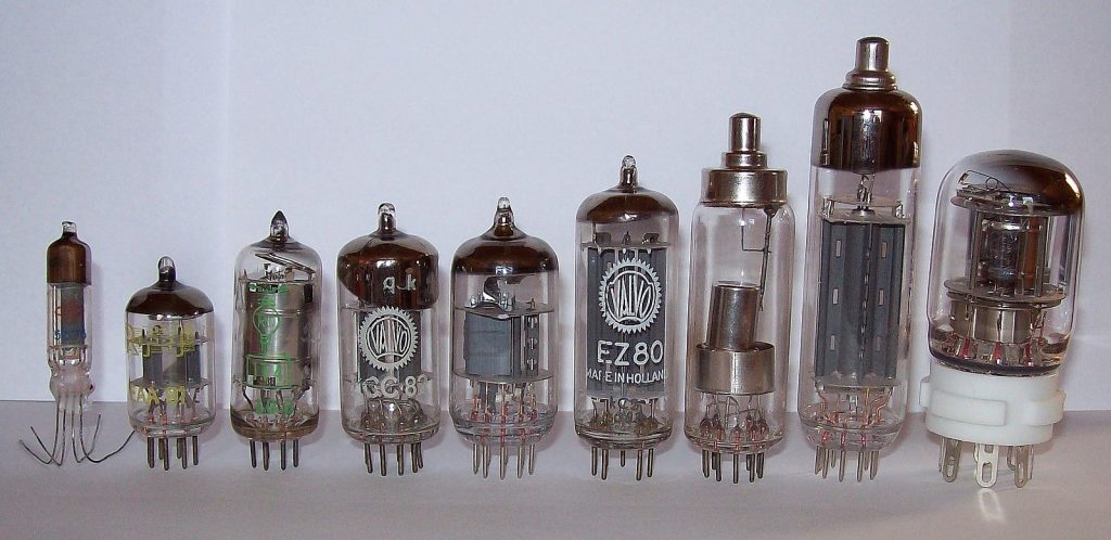
The vacuum tube
Following the discovery of the electron, we had the invention of the first practical discrete electronic device the vacuum tube in 1904.
Early vacuum tubes consisted of a metal filament a cathode (electron source) and an anode (electron receptor) plate.
The usual configuration was for the cathode to be a metal filament in the middle of the device while the anode was a metal plate surrounding the cathode.
This arrangement was then enclosed in an air-tight vacuum glass bulb.
When a current is applied to the filament, it heats up and can emit electrons through thermionic emission.
The anode is biased at a positive voltage with respect to the cathode. As such, electrons leave the heated cathode and are absorbed by the anode.
Electrons can’t leave the anode and flow to the cathode. This is because the anode is positive with respect to the cathode and it is not heated so thermionic emission does not occur.
This type of two-terminal vacuum tube was called a diode. It only allowed electrons (and hence current) to flow through it in one direction only.
This meant this device could be used to rectify signals. Vacuum tubes used as rectifiers provided an excellent way to convert alternating current (AC)to direct current (DC) as well as a stable means for detecting amplitude modulated radio waves.
In order to further improve the properties of the diode, the triode was introduced.
This featured a metal grid placed between the cathode and the anode.
If the grid is biased so that it is more negative with respect to the cathode, the negative electric field it creates around the cathode inhibits the flow of electrons to the anode.
In this arrangement, it is possible for a small change in the grid voltage to result in a large change in the current flowing from the cathode to the anode. Practically, this meant the triode could be used to amplify signals.
Together with the diode, they were used to obtain devices which enabled long-distance communication using radio waves.
Now even though vacuum tubes had their advantages, they were damaged really easily and had to be replaced frequently.
In addition, they were also quite bulky meaning electronic devices from the early 20th century were bulky and power hungry.
A better alternative was needed. So the era of vacuum tubes was soon replaced by that of discrete solid state semiconductor components.
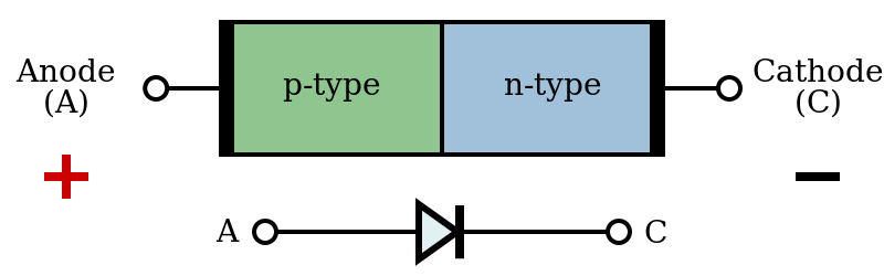
The p-n junction
The semiconductor analogue of the vacuum tube diode – the p-n junction was invented in the 1940s. This is made of a p-type semiconductor material joined to an n-type semiconductor.
A p-type semiconductor is a normal semiconductor say silicon which has been doped with a trace amount of electron acceptor element (e.g. boron). A p-type semiconductor has an excess of electron vacancies or holes.
On the other hand, an n-type semiconductor is typically pure silicon material doped with trace amounts of electron donor material (e.g. phosphorus). An n-type semiconductor has an excess of electrons.
When both p-type and n-type semiconductors are put together to form a p-n junction, a depletion layer is formed at the interface between both materials.
The depletion layer results as the electrons closest to the interface move from the n-type and recombine with the holes in the p-type.
Now if an external source say a battery is connected to the p-n junction, some interesting things happen.
The p-n junction is said to be in forward bias when the p-type and n-type sides are connected to the battery’s positive and negative terminals, respectively.
In this configuration, the positive terminal of the battery “pushes” the positively charged holes in the p-type semiconductor to cross the depletion layer.
At the same time, the negative terminal of the battery pushes the negatively charged electrons in the n-type semiconductor to also cross the depletion layer.
If the battery can push past a certain threshold value, then a current can flow in the circuit.
On the other hand, the p-n junction is said to be in reverse bias when the p-type and n-type sides are connected to the battery’s negative and positive terminals, respectively.
This configuration doesn’t allow for a current to flow in the circuit.
Accordingly, a p-n junction only allows the flow of a current in one direction only.
This is the same behaviour seen with vacuum tube diodes except this time the diode device was made a lot smaller and more power efficient.
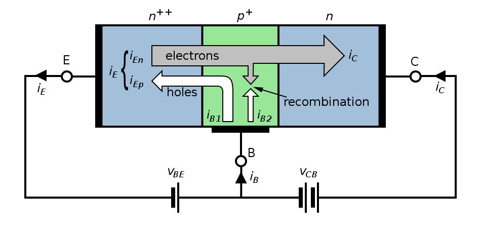
The transistor
The solid-state equivalent of the vacuum tube triode is the transistor.
Transistors are the basic building block for switching and amplification in electronic circuits. The transistor has witnessed a tremendous evolution since its invention in 1947.
In rather simple terms, a transistor consists of two p-n junctions arranged in a clever manner.
In the previous section, I explained how a p-n junction works to achieve its rectifying function. These same ideas are useful for understanding how a transistor works.
The transistor is similar to the vacuum tube triode since it also has 3 terminals. The terminals are called the emitter, base and collector. The emitter and collector are usually made of the same type of material (n-type or p-type).
The base is made of the other type of material with light doping and sandwiched between the emitter and collector.
The base is made much thinner than both the emitter and collector. So we can have two types of transistors – npn or pnp.
_jP.svg)
The emitter is doped to a much higher concentration than the collector. For simplicity going forward, I explain how an npn transistor works.
The most useful configuration is the one where the base-emitter p-n junction is forward biased while the base-collector p-n junction is reverse biased i.e. the p-type base is at a more positive voltage than the n-type emitter AND the n-type collector is at a more positive voltage than both the p-type base and the more heavily doped n-type emitter.
Given that the base-emitter p-n junction is in forward bias, electrons are “pushed” from the highly doped emitter into the base.
Since the base is thin and the collector is more lightly doped than the emitter and at a higher voltage, the electrons reaching the base-collector interface are swept into the collector.
Now, remember the p-n junction doesn’t conduct in reverse bias. So electrons can’t leave the n-type collector to enter the base.
In this way, it is possible for a small current applied to the base to control a much larger current flowing from the collector to the emitter.
As such we understand how the transistor can be used as a switch (e.g. in a logical on/off or high/low manner) or as an amplifier. The discrete bipolar transistor is superior to the vacuum triode.
It is much more compact and consumes less energy. The very first transistor (pictured above) was quite huge. It was obviously made by hand.
In the years following its invention, attempts at mass production yielded quite modest results. The breakthrough came in 1960 with the invention of metal-oxide-semiconductor field-effect transistor (MOSFET) technology.
MOSFETs are planar transistors built in one block. This means there is no need for wires connecting the transistor’s terminals.
The first MOSFETs had critical dimensions of 20 microns. MOSFETs are attractive because they can be scaled down, consume less power and they are suitable for mass production.
The most advanced MOSFETs in production in 2021 are known as fin field-effect transistors (FinFETs). FinFETs have critical dimensions equal to a few tens of nanometers.
As an example, today’s most advanced FinFETs from TSMC’s 7-nanometer technology node are so small you can ‘pack’ billions in a single chip. These FinFETs are included in common consumer electronic devices e.g. in the iPhone 12.
Future generations of transistors are foreseen to follow the trend of the last 40 years and reduce critical dimensions further.
All this means it is possible to ‘pack’ more and more transistors per chip in each new iteration of transistor technology.
Since transistors are key switching and amplification elements in electronic circuits, increasing their number means increased computational capacity.
Hence, each new iteration of transistor technology has yielded chips which are more powerful and cheaper (at least per unit) than their predecessors.
The increase in computational power and the reduced cost of chips over time is the embodiment of Moore’s law. Moore’s law holds that the number of transistors in a computer chip should double roughly every two years.
This is great news for us consumers. We always want devices with more connectivity, better reliability and cheaper costs.
The growth of the internet is an excellent example of how customer behaviour and expectation is pushing the electronics and photonics industries.
The internet as the driving force behind advances in photonics and electronics
The internet is a central feature of our lives. We use it to share all kinds of emotions. It is ever present in all spheres of our lives.
No matter what we use it for e.g. business, entertainment, education or just staying, one thing is sure.
We always want more bandwidth to access content online faster. The recent covid-19 pandemic further accelerated demand for more data as we were holed up in our homes and making lots of video calls on a daily basis.
You can get an idea of the current situation by looking at the amount of data created on the internet every minute.
For example, this year we have 500 hours worth of content uploaded to Youtube every minute. This is a staggering amount of data.
For context, we note that in 2015 we only had 30 hours of video content uploaded to Youtube every minute.

In a utopic world, Moore’s law would go on forever. However, in the real world we will eventually reach a physical limit where transistors are only atoms thick.
We can’t change the laws of physics and make transistors smaller than individual atoms. As electronics runs out of steam, we need to find alternatives in order to keep on delivering on the promise of Moore’s law.
There is an urgent need to keep on scaling and delivering faster interconnectivity.
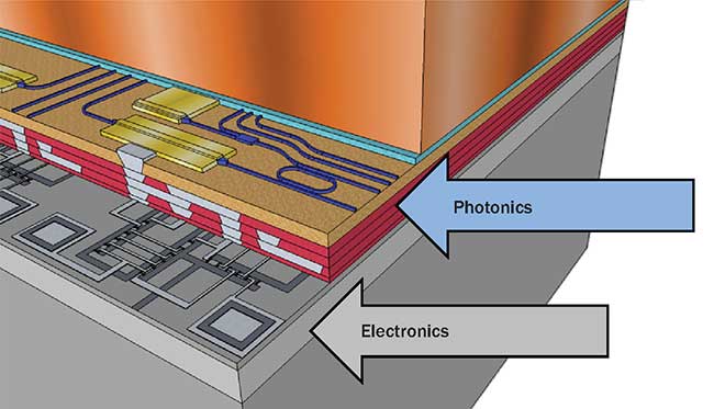
Everything is lining up for photonics to take the mantle over from electronics and continue Moore’s law. Photonics is already following in the footsteps of electronics.
In 40 years, it has witnessed a tremendous amount of integration. From discrete components like lenses, optical fibres and detectors, it has evolved into systems which can generate, modulate, re-route and detect light in a single chip.
Manipulating light signals is more complicated than working with electrons. I will not include an extensive explanation of the evolution of photonics technology.
For that, you would have to check out our article on photonics – the technology of light.
Will photonics replace electronics?
In my opinion, I think photonics will definitely replace electronics in the coming years. It is just a matter of when and not if.
However, electronics has a long track record and a lot of money has been invested into it.
So the most reasonable thing to do is to start with hybrid systems integrating both photonics and electronics.
Photonics functionality will augment electronics to realise new functions and increase speed/bandwidth.
Next, the electronic parts of integrated circuits will be phased out one by one until we have fully photonic integrated circuits.
The relationship between photonics and electronics is akin to that of siblings. Both fields are quite similar in their goals except the fundamental “messenger” particles are electrons in one case and photons in the other.
Despite the difference in messenger, information propagates as electromagnetic waves in both electronics and photonics.
Photonics is basically following electronic’s playbook. Just like electronics, photonics started out with discrete, bulky and expensive components.
It has slowly evolved (and will continue to do so for the foreseeable future) to include more integration.
From systems with lenses, optical fibres, prism splitters etc we are already seeing PICs with laser sources, modulators, filters, switches, waveguides and detectors on the same chip.
Advantages of photonics over electronics
Despite their similarities, I think there are three reasons which can help us understand why photonics will supersede electronics;
1. Integrated photonics doesn’t require heavy capital investments
Switching from one technology to another doesn’t always have to do with technical superiority. More often than not, economics plays a big part in deciding which technology wins.
In this respect, photonics has a trump card it can always play to tip the scales.
Photonic integrated circuits (especially silicon photonics) can be fabricated using the same foundries which already manufacture electronic chips.
This means the switch from electronic integrated circuits to photonic integrated circuits will not require a costly overhaul of manufacturing equipment.
This is a serious advantage for photonics because building a new foundry plant usually costs several billion.
Additionally, photonics doesn’t require the same critical dimensions as advanced electronics. Current electronics manufacturing is at a technology node with critical dimensions on the order of a few tens of nanometers.
Since light is zoomed around photonics chips to achieve useful stuff, you need the waveguides to be somewhat comparable to the wavelength of the light.
As such more mature technology nodes like the 130-nanometer technology node are more suitable for integrated photonics.
It is also important to note that for photonics the roughness of waveguide sidewalls is more important.
Light travelling in a waveguide is very sensitive to surface imperfections which can cause unwanted reflections or refractions thereby leading to power losses.
The more advanced technology nodes used for electronics do allow for greater control in dimensions and smoothness.
This know-how can be brought to the more mature nodes in order to optimise them for photonics.
2. Photonics has a much higher data capacity than electronics
Photonics has a significantly higher data capacity than electronics. The carrier of information in photonic and electronic circuits is the same – electromagnetic waves.
In a vacuum, electromagnetic waves travel at a speed of 300 thousand kilometres per second.
In electronics, the medium for transmission of information is a metal wire (usually this metal is copper) at the network level or a metal trace for integrated circuits.
In photonics, the medium for transmission is a glass optical fibre at network level. For photonic integrated circuits, the materials of choice are either silicon or indium phosphide.
In electronics, we are usually dealing with radio waves whereas in photonics, we work with visible or near-infrared light.
This means in electronics we will typically deal with frequencies in the kilohertz (KHz), megahertz (MHz) or gigahertz (GHz) ranges.
On the other hand, for photonics we are dealing with frequencies in the terahertz (THz) regime.
For radio waves, the speed of the wave travelling on a copper wire is significantly less than the speed in a vacuum. The speed of radio waves in copper depends on its permittivity and conductivity.
These parameters can also be frequency dependent so this can make things rather complex. As an example, radio waves at GHz frequencies can have a speed of about 30 kilometres per second.
For light travelling in optical fibres, indium phosphide or silicon there is almost no loss.
The only losses which occur are due to small trace impurities in the bulk of the material or imperfections at the surface of the optical fibre or waveguide.
The materials typically used for photonics are dielectrics.
Usually, these systems are engineered such that the frequency of the light used in them falls within their transparency windows.
The speed of light in a dielectric is equal to the speed of light in vacuum divided by its refractive index. In glass this corresponds to 200 thousand kilometres per second.
In silicon, light travels at a speed of 87 thousand kilometres per second.
The best electronic circuits can achieve data transfer speeds ranging from 5 to 12 gigabytes per second (GBps).
In contrast, photonic integrated circuits can already reach speeds of 3 to 5 GBps. So far so good for electronics.
However, with photonics, it is possible to use several different laser signals at slightly different wavelengths as separate data channels.
This technique is called wavelength division multiplexing.
You can line up several different wavelength channels on the same physical channel and thus boost data transmission speeds to the hundreds of gigabytes per second and eventually reach the terabyte per second (TBps) range.
3. Photonics is multidisciplinary
Photonics is an acutely multidisciplinary discipline. Sure electronics has had a huge impact on our society.
It has found its way into many different industries. Photonics is set to simply blow it out of the water though.
Photonics can offer the data speeds needed to accommodate our video and data-hungry society. In so doing it will help create more applications we can’t even imagine today.
Photonics is a key ingredient in several forward-looking technologies like 5G for telecom, the internet of things (IoT), autonomous driving (through LIDAR), bio-photonics, sensor technology, medicine, high-performance computing and quantum computing.
The advances and gains in photonic integrated circuits would spill over to several different sectors. Even those sectors we don’t immediately think of will benefit enormously from photonics.
For example, photonics will seriously boost data science and analytics as it is set to make tons of data available for things like machine learning or just simply making inferences.
Conclusion
So far we have taken a deep dive into the fascinating relationship between photonics and electronics. In many ways, electronics is today’s technology.
It is mature with advances in processing technology over the last 60+ years resulting in a tremendous increase in computing power with reducing cost.
On the other hand, photonics is tomorrow’s technology. Current photonics technology is barely 40 years old.
Despite its “youthfulness”, it is already challenging electronics and it is still a long way off from achieving its full potential.
One area where we see this perspective quite clearly is that of data transfer rates.
After 60 years of progress, the most sophisticated electronic circuits can achieve data transfer speeds of up to 12 GBps.
From all indications, future electronics systems will not be able to substantially surpass this speed.
Future advancements in electronics are set to focus on producing bespoke ICs tailored to the unique requirements of each application.
In contrast, photonic circuits can already offer speeds is set to offer data transfer speeds which are well in excess of the best electronics can offer.
Now even though photonics will eventually replace electronics, I don’t think it makes sense to think of both technologies as competitors.
Their relationship is indeed fascinating because it is a win-win scenario.
Developments in electronics help push photonics forward and vice-versa.
Nano/microelectronics and photonics are key emerging technologies which form the basis for future technological advancement.
They affect every other industry, so progress in this field has a positive knock-on effect on the other technology sectors.